1. 182mm wafer VS 210mm wafer
Advantages of 210 silicon wafers:
①The increasing size of silicon wafers can bring about cost reduction and efficiency gains in many aspects of the downstream process. Large wafer cost reduction mainly comes from the “flux” and “inconsistent area perimeter increase” cost reduction effect.
Flux: the capacity increases when the silicon wafer becomes larger, and the corresponding equipment, manpower, etc. do not need to increase the cost reduction effect. In the cell segment, the production rate of the cell line is calculated in wafers. When the wafer area becomes larger, the cell capacity increases accordingly, which brings the dilution of labor, depreciation, and three costs, etc. M12 cells can save 0.08 Yuan/W compared to M2 cells, a 25.6% reduction. The module segment is similar, with the increase in capacity bringing dilution of labor and depreciation.
Area increase: mainly in the module side and end power station. That is, when the wafer and module size becomes larger, the amount of bezel, welding tape, etc. increases accordingly. However, the increase is smaller than the increase in size and area, and the resulting cost per watt can be saved. This effect is mainly reflected in the module side of the bezel, and welding tape. This effect is mainly reflected in the bezel and welding tape at the module end, as well as the bracket for the end power plant.
②Whether it is N-type cell technology, or stacking with calcium titanium ore, the future is based on 210.

Disadvantages of 210 silicon wafers (=advantages of 182 silicon wafers):
Existing capacity cannot be upgraded from 156 to 210 through technical reform, while Perc cells have been caught in a fierce price war. In such a market environment, cell makers have insufficient incentive to add new cell capacity. Therefore, in the short term, the large-scale industrial application of 210 wafers cannot be realized for the time being. Suitable for new plants to expand production to buy new equipment to use 210 wafers.
Conclusion: One strives for the present and the other looks to the future.
It can be said that these two are one striving for the present and one looking at the future. They are not good or bad but will be absorbed by the times when they follow the historical trend. The future is expected to lead to a new wave of innovation in the PV industry with the widespread use of large silicon wafers.
2. Semiconductor wafers VS PV wafers
Both are made of monocrystalline silicon.
Photovoltaic silicon wafers
The requirements for parameters such as purity and warpage are low, and the manufacturing process is relatively simple.
Take monocrystalline silicon cells as an example:
The first step is to cut and round the square. First, the monocrystalline silicon rods are cut into square rods according to the size requirements, and then the four corners of the square rods are rounded.
The second step is pickling, which is mainly to remove impurities from the surface of the monocrystalline square rod.
The third step is slicing, where the cleaned square rods are first glued to the workboard. Then the work plate is placed on the slicer and cut according to the process parameters that have been set.
Finally, the monocrystalline wafers are cleaned and monitored for surface smoothness, resistivity, and other parameters.
Semiconductor Silicon Wafers
Semiconductor silicon wafers are more demanding than PV wafers. First of all, all silicon wafers used in the semiconductor industry are monocrystalline silicon. The purpose is to ensure the same electrical characteristics of each bit of silicon wafer. In terms of shape and size, monocrystalline silicon wafers for photovoltaics are square. They are mainly available in 125mm, 150mm, and 156mm side lengths. Monocrystalline silicon wafers for semiconductors are round, with wafer diameters of 150mm (6″ wafers), 200mm (8″ wafers) and 300mm (12″ wafers).

In terms of purity, the purity of monocrystalline silicon wafers for photovoltaics requires a silicon content of between 4N and 6N (99.99%-99.9999%). However, monocrystalline silicon wafers for semiconductors are around 9N (99.999999999%) to 11N (99.999999999%), requiring a minimum purity of 1000 times that of PV monocrystalline silicon wafers. Therefore, the purity of semiconductor wafers is much higher than that of photovoltaic wafers.
In terms of appearance, the surface flatness, smoothness and cleanliness of semiconductor wafers are higher than those of PV wafers. Purity is the biggest difference between monocrystalline silicon wafers for photovoltaics and monocrystalline silicon wafers for semiconductors.
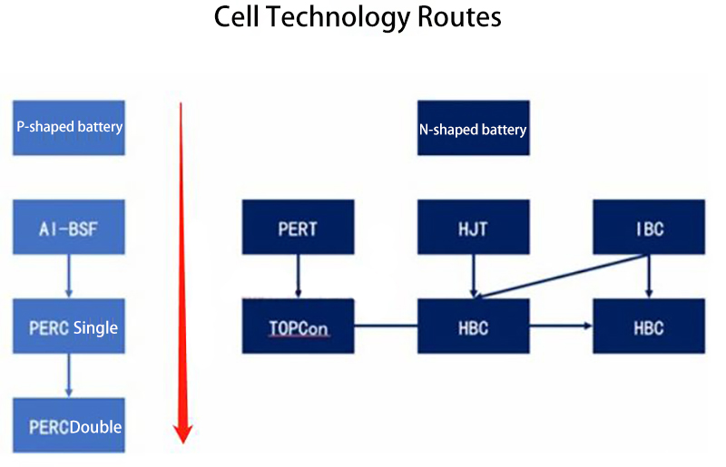
3. P-type cells VS N-type cells
The future is the world of N-shaped batteries.
Advantages of N-type cells over P-type cells.
(1) High conversion efficiency. Currently, the average mass production efficiency of PERC stacked with SE technology is 22%-22.4% for P cells, 22.4%-23.1% for TOPCon, and 23%-23.6% for HJT in N cells.
(2) High bifacial rate. P-type PERC cell bifacial rate is about 75%, while N-TOPCon bifacial rate is over 85% and N-HJT bifacial rate is over 95%.
(3) Low-temperature coefficient, N-type cell temperature coefficient is lower than P-type, suitable for higher temperature application scenarios such as Africa, the Middle East, and other regions with better irradiation conditions.
-
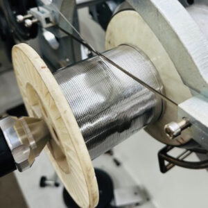
 0.9*0.22 mm PV Tabbing Ribbon for Solar PV Modules
 - 0.6*0.18 mm PV Tabbing Ribbon for Solar Panel
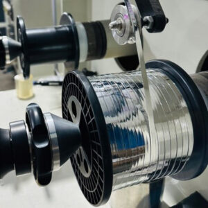
- 1.1*0.18 mm PV Tabbing Ribbon for Solar Modules
- 5*0.35 mm PV Busbar for Solar PV Modules
- 3*0.35 mm PV Busbar for Solar Modules
- 3.5*0.35 mm PV Busbar for Solar Panel
- 1*0.18 mm PV Tabbing Ribbon for Photovoltaic Modules
- 4*0.35 mm PV Busbar for Photovoltaic Modules